2023 2024 Student Forum > Management Forum > Main Forum

 
  #2  
1st August 2015, 11:28 AM
Super Moderator
 
Join Date: Mar 2013
Re: EEE Paper RTU

As you want I am here giving you sample paper of Advanced Power electronic subject of B.Tech EEE program of Rajasthan Technical University(RTU).

Sample paper :

Unit-I

Q 1. (a) Analyse the output waveform of a single phase a.c. regulator ( converter) into various harmonics with Fourier series and find the expression for the amplitude of nth harmonic, Enm and its phase Φn. [8]
(b) A 3-Φ, 3 wire bidirectional controller supplies a star-connected R load of R = 5Ω and the line-to-line input voltage of 210v (rms) at 50Hz. The firing angle α=π/3 Determine.
(i) rms output-phase voltage, Eo
(ii) input power factor, P f , and
(iii) expression for the instantaneous output voltage of phase a. [8]
OR
Q2. (a) Discuss the Operation of a 1 - Φ AC controller with RL load, when the firing angle α, is less than, or equal to, load phase angle Φ. Also, show that for a less than Φ, the output voltage of the AC controller cannot be regulated. . [8]
(b) A single - phase half-wave AC controller of given figure feeds power to a resistive load of 6Ω from 230 V, 50 Hz source.
The firing angle ofSCR is π/2 . Calculate.
(i) rms value of output voltage
(ii) input power factor
(iii) average input current [8]

Unit - II

Q3. A 3-Φ bridge inverter is operated is 1800 conduction mode. Draw the output line voltage waveforms and obtain:
(i) Fourier series for the line voltage.
(ii) RMS value of nth harmonic-line voltage.
(iii) RMS value of fundamental component of line voltage.
(iv) RMS value of line voltage.
(v) Distortion and harmonic factor. [16]
OR
Q4. (a) What is the need for controlling the output at the output terminals of an inverter? Also, Discuss briefly and compare the various methods employed for the control of output voltage of inverters. [8]
(b) A capacitor commutated 1-Φ bridge inverter is operated at 50Hz with resistive load of 5Ω. Thyristor turn-off time is 62µ sec. Find
(i) Commutating Capacitor 'C' for successful commutation of,SCR.
(ii) Load current
(iii) F critical
(iv) R critical [8]

Unit - III

Q5. (a) A 3-Φ to 1-Φ cycloconverter employs a three pulse positive and negative group converters. Each converter is supplied from delta/star transformer with per phase turns ratio of 3:1. The supply voltage is 410V, 50 Hz. The load RL has R = 4Ω and at low output frequency, WoL = 3Ω. The commutation overlapand thyristor turn-off time, limits the firing is inversion mode to 160° For this, Calculate :
(i) the value of fundamental RMS output voltage
(ii) RMS output current
(iii) Output power [10]
(b) Draw and explain the control circuit block diagram for a cycloconverter with non-circulating current mode. [6]
OR
Q6 (a) Discuss why a 3-Φ to l-Φ cycloconverter requires positive and negative group phase-controlled converters. Under what conditions, the group works as inverter or rectifier? How should the firing angles of two convertors can be controlled? [10]
(b) A 3-Φ cyloconvertor feeds a 1-Φ load of 190 V, 45 A at power factor of O. 7 (lagging). Determine:
(i) the required supply voltage
(ii) thyristor rating, and
(iii) power faetor of supply current [6]

Unit - IV

Q7. (a) Derive an expression for voltage transfer ratio Vo/V s in terms of transformer turns ratio and duty cycle for flyback converter, operating with continous load current. [8]
(b) Explain the operation of Resonant - DC power supply. [8]
OR
Q8. (a) With a neat sketch, explain the operation of forward converter and derive the equation for its output voltage. [8]
(b) Wirte a short note on : - [8]
(i) Switch mode DC power supplies
(ii) Bi-directional power supplies

Unit - V

Q9. (a) Discuss the operation of bidirectional AC power supplies. [8]
(b) Discuss multistage converter used for the conditioning of power factor. [8]
OR
Q10. The load resistance of ac power supplied in the given figure is R =1.5 Ω. The dc input voltage is Vs = 24V. The input inverter operates at a frequency of 400 Hz with a uniform PWM of eight pulses per half-cycle & the width of each pulse is δ = 20°. The ON-state voltage drops of transistor switches & diodes are neglected. Turns ratio of transformer is 4. Determine rms load current. Neglect the losses in T/F and effect of load on resonant frequency. [16]
  #3  
14th May 2020, 08:19 AM
Unregistered
Guest
 
Re: EEE Paper RTU

Can you provide me the Syllabus for B. Tech (Electrical & Electronics Engineering), 3rd semester offered by RTU (Rajasthan Technical University) on which the question paper is based?
  #4  
14th May 2020, 08:22 AM
Super Moderator
 
Join Date: Aug 2012
Re: EEE Paper RTU

The Syllabus for B. Tech (Electrical & Electronics Engineering), 3rd semester offered by RTU (Rajasthan Technical University) on which the question paper is based is as follows:


3EX1A: ELECTRONIC DEVICES & CIRCUITS (Common to EE, EX, EC and EI)

1
Semiconductor Physics: Mobility and conductivity, charge densities in a semiconductor, Fermi Dirac distribution, Fermi-Dirac statistics and Boltzmann approximation to the Fermi-Dirac statistics, carrier concentrations and Fermi levels in semiconductor.

Generation and recombination of charges, diffusion and continuity equation, transport equations, Mass action Law, Hall effect.


2
Junction Diodes: Formation of homogenous and hetrojunction diodes and their energy band diagrams, calculation of contact potential and depletion width, V-I characteristics, Small signal models of diode, Diode as a circuit element, diode parameters and load line concept, C-V characteristics and dopant profile.

Applications of diodes in rectifier, clipping, clamping circuits and voltage multipliers Transient behavior of PN diode Breakdown diodes, Schottky diodes, and Zener diode as voltage regulator Construction, characteristics and operating principle of UJT


3
Transistors: Characteristics, Current Components, Current Gains: alpha and beta. Variation of transistor parameter with temperature and current level, Operating point, Hybrid model, DC model of transistor, h-parameter equivalent circuits.CE, CB and CC configuration


DC and AC analysis of single stage CE, CC (Emitter follower) and CB amplifiers AC & DC load line, Ebers-Moll model Biasing & stabilization techniques Thermal runaway, Thermal stability


4
JFET & MOSFET: Construction and operation of JFET & MOSFET, noise performances of FET, parasitic of MOSFET, small signal models of JFET & MOSFET.

Biasing of JFET's & MOSFET’s Low frequency single stage CS and CD (source follower) JFET amplifiers.FET as voltage variable resistor and active load


5
Small Signal Amplifiers at Low Frequency: Analysis of BJT and FET multistage amplifier, DC and RC coupled amplifiers. Frequency response of single and multistage amplifier, mid-band gain, gains at low and high frequency.

Analysis of DC and differential amplifiers, Miller's Theorem, use of Miller and bootstrap configuration Cascade and cascade configuration of multistage amplifiers (CE-CE, CE-CB, CS-CS and CS-CD), Darlington pair


Syllabus B. Tech (EEE), 3rd semester Rajasthan Technical University
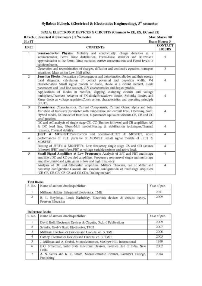


Quick Reply
Your Username: Click here to log in

Message:
Options


All times are GMT +5. The time now is 12:19 AM.


Powered by vBulletin® Version 3.8.11
Copyright ©2000 - 2024, vBulletin Solutions Inc.
SEO by vBSEO 3.6.0 PL2

1 2 3 4