|
#2
11th December 2014, 01:49 PM
| |||
| |||
| Re: IIT Bombay M.Tech VLSI Designing Course Details
The Indian Institute of Technology Bombay is located at The Indian Institute of Technology Bombay . •The largest Department at IIT •About 40 faculty and 600 students •Major research and teaching –Communications & Signal Processing–Power Electronics & Power Systems–Electronic Systems–Control & Computing–Microelectronics & VLSI Facilities: •Class 1000 Clean Room (class 100 work areas) with facilities for complete IC manufacturing (optical & EB lithography, RIE, Deposition, Sputter, RTP, Furnace facilities) •MEMS fabrication •Excellent characterization facility •SEM; photoluminescence •VLSI design workstations •VLSI design tools–Cadence, Mentor, Synopsys, Tanner, Xilinx, plus many public domain tools •Simulation workstations •Simulation software–Medici, TSuprem, ISE-TCAD, SMC (Monte Carlo) •GaitondeIntegrated Systems Laboratory •Intel Microelectronics Lab •TCS VLSI Design Lab 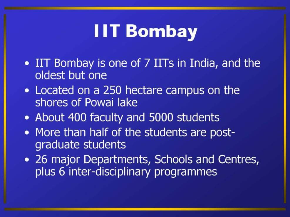 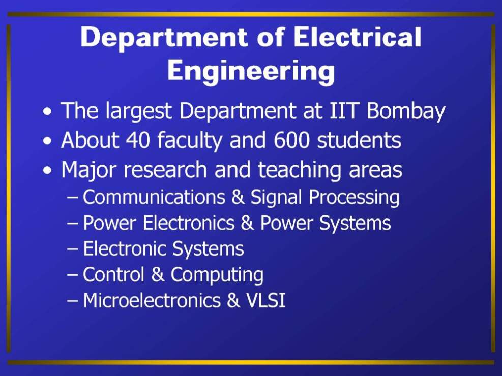 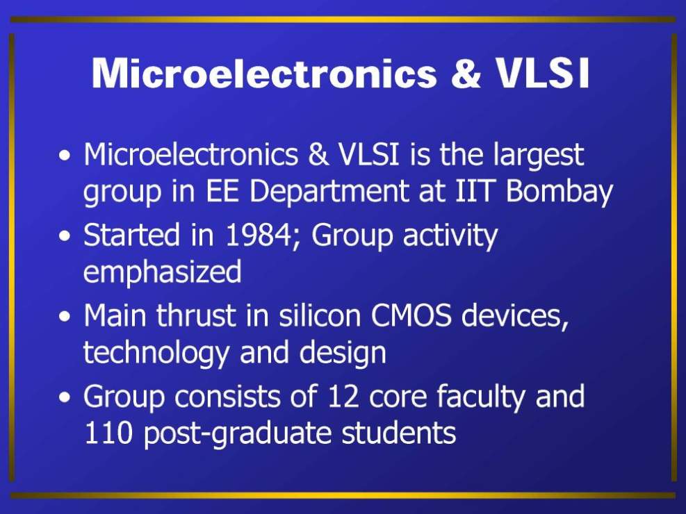    For detailed information , here is the attachment Contact Details •Microelectronics Group Department of Electrical EngineeringIndian Institute of Technology, BombayPowaiMumbai 400076 India •Phone: +91-22-2572-3655 •Fax:+91-22-2572-3480 |