#1
26th June 2015, 08:20 AM
| |||
| |||
EDC Mumbai University
I am the student of Information Technology (I.T) Engineering Semester 3 of the Mumbai University and I need the last year question paper of the Electronic Device and Circuits (EDC) subject for the preparation so can you please provide me this?
|
#2
4th November 2015, 01:28 PM
| |||
| |||
Re: EDC Mumbai University
I would like to have the Mumbai University IT II Year III Semester Electronic Device and Circuits Question Papers
|
#3
4th November 2015, 01:29 PM
| |||
| |||
Re: EDC Mumbai University
Mumbai University IT II Year III Semester Electronic Device and Circuits Question Paper N.B.: (1) Question NO.1 is compulsory. (2) Attempt any four questions out of rernainln!:l six questions. (3) Assume suitable data if necessary. (4) Figure to the right indicate full marks. 1. (a) State and explain Barkhusen’s Criterion for oscillator. (b) Obtain the expression for the collector current of a x’ster in CE configuration. (c) Draw the Ckt diagram and explain the operation of Dua! input unba.lanced output A differential amplifier. 2. (a) With the help of Block diagram explain operation of practical inverting ampli~ier. (b) Draw the C.kt diagram and explain operation of wienbridge oscillator. (c) Explain different external compensation tech. 3. (a) Derive the frequency respoAse of a practicaldifferentiator and explain it’s working. 10 (b) Draw the ~ypical connection diagram of VCO using IC 566. State the expression 10 for the•output frequency how the output frequency can be changed. 4. (a) A 6 bit OAC has an input 100101 and 10V reference voltage find :- (i) Output voltage (ii) Conversion .f~solutfon . ‘(b) Design a regulator using IC – 723 to meet the following specification 10 ‘V o = 5V. 10 = 100 mAt Vin = 15 ± 20%Isc= 150 mA, VsensA= 0•7 V. 5.(a) Draw the Ckt diagram and explain the operation of monostable multivibrator. 10 (b) Deriv.e the expressiofl for stability factor ‘S’for different BJT Biasing Ckt. 10 6. (a) What is a notch filter? Explain it’s operation with the help of neat Ckt diagram. 10 ‘(b) Draw the Ckt diagram and explain the operation of triangular wave generator 10/’using OP-AMP. 7. (a) Write program for SPICE simulation of non-inverting amplifier. 10 (b) Explain various circuits used to provide constant current bias in a differential |
#4
15th February 2016, 11:20 AM
| |||
| |||
Re: EDC Mumbai University
Hii Guys , Here I am Looking for B. tech Electrical Engineering Previous year III Semester Electronic Device and Circuits Question Papers of Mumbai University , Will you please Provide me Same for my help ?
|
#5
15th February 2016, 11:23 AM
| |||
| |||
Re: EDC Mumbai University
Friend Have a Look , I am Providing III Semester Electronic Device and Circuits Question Paper of Mumbai University : Question NO.1 is Compulsory. Attempt any four Questions out l Six Questions. Assume suitable data if necessary. Figure to the right indicate full marks. 1. (a) State and explain Barkhusen’s Criterion for oscillator. (b) Obtain the expression for the collector current of a x’ster in CE configuration. (c) Draw the Ckt diagram and explain the operation of Dua! input unba.lanced output A differential amplifier. 2. (a) With the help of Block diagram explain operation of practical inverting ampli~ier. (b) Draw the C.kt diagram and explain operation of wienbridge oscillator. (c) Explain different external compensation tech. 3. (a) Derive the frequency respoAse of a practicaldifferentiator and explain it’s working. 10 (b) Draw the ~ypical connection diagram of VCO using IC 566. State the expression 10 for the•output frequency how the output frequency can be changed. 4. (a) A 6 bit OAC has an input 100101 and 10V reference voltage find :- (i) Output voltage (ii) Conversion .f~solutfon . ‘(b) Design a regulator using IC – 723 to meet the following specification 10 ‘V o = 5V. 10 = 100 mAt Vin = 15 ± 20%Isc= 150 mA, VsensA= 0•7 V. 5.(a) Draw the Ckt diagram and explain the operation of monostable multivibrator. 10 (b) Deriv.e the expressiofl for stability factor ‘S’for different BJT Biasing Ckt. 10 6. (a) What is a notch filter? Explain it’s operation with the help of neat Ckt diagram. 10 ‘(b) Draw the Ckt diagram and explain the operation of triangular wave generator 10/’using OP-AMP. 7. (a) Write program for SPICE simulation of non-inverting amplifier. 10 (b) Explain various circuits used to provide constant current bias in a differential For Complete Previous year III Semester Electronic Device and Circuits Question Paper I am Sharing Image of this page 
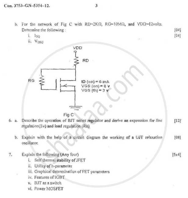
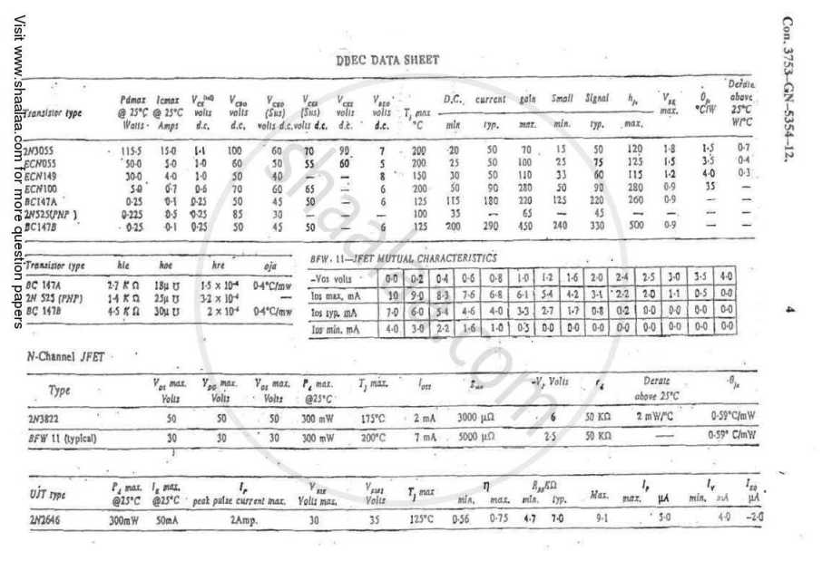
Contcat No : 022 2654 3000 Address : University Of Mumbai CST Road, Kalina, Santacruz East Mumbai, Maharashtra 400098 |
|