|
#3
19th April 2018, 06:44 PM
| |||
| |||
| Re: DPSD Anna University Question Papers
As you want to download question paper of Digital Principles and System Design (DPSD) Subject of B.Tech Course of Anna University, so here I am providing question paper: Anna University Digital Principles and System Design (DPSD) Question Paper PART A - (10 2 = 20 Marks) 1. Represent the decimal numbers -200 & 200 using 2s complement binary form. 2. Write the truth table of AND and XOR gates. 3. Draw the schematic of half adder logic. 4. Write the HDL descriptor of following circuit. 5. Determine the size & number of multiplexers required to implement the full adder. 6. Determine the no of address lines required for 512 bytes of memory and for 2kb memory. 7. Write state transition diagram of JK Flip-flop. 8. Draw the timing diagram showing the output of a 2 stage synchronous counter with respect to its clock signal. 9. Explain the next state characteristics of D and SR flip-flops. 10. Define static and dynamic hazards. PART B-(5 16 = 80 Marks) 11. (a) (i) Convert (1947)10 into its equivalent octal and decimal representation (10) (ii) Perform (147-89) using 2s complement binary arithmetic. (6) (Or) (b) (i) Minimize the following expressions using K-Map Y= A'BC'D' + A'BC'D + ABC'D' + AB'C'D +A'B'CD'. (10) (ii) State and prove De Morgans theorems (6) 12. (a) (i) Design a combinational circuit that comprises only of NOR gates for the following expression giving the input & output relation. Y=ABC + AC +B ' C (10) (ii) Draw the schematic of full adder and give its truth table. (6) (Or) (b) (i)Design a BCD to Excess-3 code converter using truth table & K-Map simplification. (10) (ii) Draw the schematic of a magnitude comparator and give its truth table. 6) 13. (a) (i) Design a combinational logic using a suitable multiplexer to realize the Boolean expression Y=AD ' + B'C + BC'D (10) (ii) Compare and contrast encoders & multiplexers (6) (Or) (b) (i) Write short notes on the basic configuration of the 3 types of programmable logic devices. (6) (ii) Draw the signals of a 32 x 8 RAM with control input. Show the external connections necessary to have a 128 x 8 RAM using a decoder and the replication of this RAM. (10) 14. (a) A synchronous counter with four JK flip- flops has the following connections: JA=KA=1, JB=QAQD , KB=QA JC=KC=QAQB JD=QAQBQC AND KD=QA Determine the modulus n of the counter and draw the output waveforms of the same (16) (Or) (b) Design a synchronous counter using JK flip-flop to count the following sequence: 1-3-15-5-8-2-0-12-6-9. (16) 15. (a) (i) Explain the working principle of switch debounce logic. (6) (ii) Determine whether the circuit is stable or not whose excitation function is given by - y=(x1y)x2 (10) (Or) (b) (i) Derive a circuit specified for the following table (10) (ii) Determine whether the following circuit has a static hazard or not. If yes, design a hazard free logic for the same input and output relation.(6) Anna University Digital Principles and System Design (DPSD) Question Paper 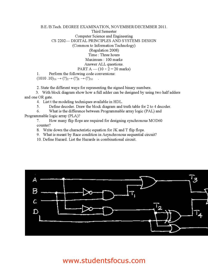 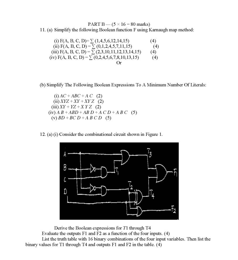 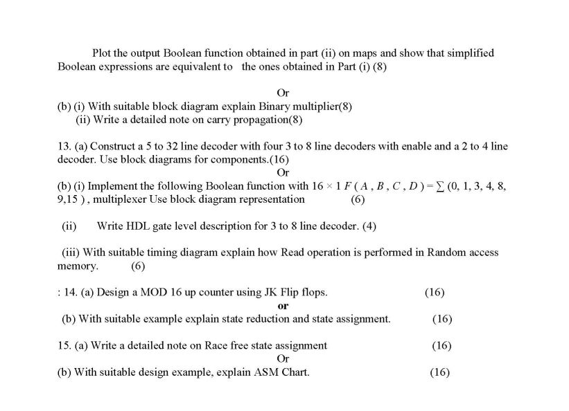 |