|
#2
19th August 2015, 09:14 AM
| |||
| |||
| Re: Jyoti Prakash Kar NIT Rourkela
As you want to get the details of profile of Jyoti Prakash Kar of National Institute of Technology Rourkela so here is the information of the same for you: Dr. Jyoti Prakash Kar Assistant Professor Department of Physics National Institute of Technology (NIT) Rourkela Odisha, India, 769008 Email: karjp@nitrkl.ac.in, jpkar@hotmail.com Phone (O):+91-6612462732 Research Interests: Thin Electronic Films, High-k Dielectrics, Microelectronics and Semiconductor Technology, Solid State Sensors and Devices, MEMS, Non-Destructive Testing, Surface Engineering, Nanotechnology Educational Profile: M. Sc. (Utkal University), M. Tech (IIT Delhi), Ph. D. (IIT Delhi) Course Offered: * Vacuum Science and Applications (PH 462) * Physics-I (PH 101) Teaching/Research Experiences: * Assistant Professor, (Dec 2011-Continuing), Dept. of Physics, National Institute of Technology, Rourkela, India * Marie Curie researcher (June 2011-Dec 2011), Dept. of Electronics Engineering, University of Tor Vergata, Rome, Italy * Postdoctoral researcher (July 2010-June 2011), Dept. of Electronics Engineering, University of Tor Vergata, Rome, Italy * Postdoctoral researcher (July 2007-June 2010), Dept. of Materials Sci. and Eng., Yonsei University, Seoul, S. Korea * Visiting researcher (Nov 2006-Apr 2007), Dept. of Electrical and Computer Eng., University of Oklahoma, Norman, USA Research Fellowship/Scholarships: * Marie Curie fellowship (June 2011-Dec 2011) * Research fellowship, University of Tor Vergata, Rome, Italy (July 2010-June 2011) * Brain Korea (BK) 21 fellowship, S. Korea (July 2007-June 2010) * Research fellowship, University of Oklahoma, USA (Nov 2006-Apr 2007) * MHRD, India scholarship during M. Tech and Research Awards/Honours: * Brain Korea 21 Annual Research Prize 2009, Dept. of Materials Science and Engineering, Yonsei University, S. Korea * Brain Korea 21 Annual Research Prize 2008, Dept. of Materials Science and Engineering, Yonsei University, S. Korea * Gold prize 2008 (Brain Korea 21), Dept. of Materials Science and Engineering, Yonsei University, S. Korea Recognition: * America’s Marquis Who’s Who in the world for 2010 edition * International Biographical Centre, Cambridge, UK (2010 edition) Membership: * Materials Research Society (MRS), 2007-2010, South Korea * Materials Research Society (MRS), 2005-2007, Singapore Reviewer of International Journals: Materials Science and Engineering B, Applied surface science, IEEE Sensors Journal, Surface Engineering, Sensor Letters, Current Nanoscience, Physica E, Materials Science in Semiconductor Processing Book/Book chapters: * Book: Acoustic Waves - From Microdevices to Helioseismology, Chapter: “Aluminum nitride (AlN) film based acoustic devices: Material synthesis and device fabrication”, J. P. Kar and G. Bose. (Intech publication 2011, ISBN: 978-953-307-572-3) * Book: Nanowires Fundamental Research, Chapter: “Junction properties and applications of ZnO single nanowire based Schottky diode”, S. N. Das, J. P. Kar and J. M. Myoung. (Intech publication 2010, ISBN: 978-953-307-327-9) * “Lead salt thin film semiconductors for microelectronic applications”, S. Mukherjee, D. Li, A. Gautam, J. P. Kar and Z. Shi. (Transworld Research Network 2010, ISBN: 978- 81-7895-501-8) Publications: Journals: 1. “Fabrication and characterization of vertically aligned long ZnO nanorods on transparent substrate”, J. P. Kar, J. H. Choi, S. N. Das, J. Xiong, M. J. Lee, T. I. Lee and J. M. Myoung, Journal of Nanoscience and Nanotechnology,11 (2011) 2185. 2. “Investigation of optical and compositional properties of thin SiN x:H films with an enhanced growth rate by high frequency PECVD method”, M. J. Lee, J. P. Kar, T. I. Lee, D. Lee, D. K. Choi, J. H. Cho and J. M. Myoung, Vacuum, 85 (2011) 1032. 3. “Growth, modulation and Photoresponse characteristics of vertically aligned ZnO nanowires”, J. P. Kar, S. N. Das, J. H. Choi, T. I. Lee, J. Seo, T. Lee and J. M. Myoung, Applied Surface Science, 257 (2011) 4973. 4. “One-dimensional semiconductor nanostructure based thin-film partial composite formed by transfer implantation for high-performance flexible and printable electronics at low temperature”, K. J. Moon, T. I. Lee, J. H. Choi, J. Jeon, Y. H. Kang, J. P. Kar, J. H. Kang, I. Yun, J. M. Myoung, ACS Nano, 5 (2011) 159. 5. “Performance enhanced carbon nanotube films by mechanical pressure for a transparent metal oxide thin film field effect transistor”, J. Jeon, T. I. Lee, J. H. Choi, J. P. Kar, W. J. Choi, H. K. Baik and J. M. Myoung, Electrochemical and Solid-State Letters, 14 (2011) H76. 6. “Self-regulating pseudo-monolayer printing of percolating networks of ZnO nanostructures for macroelectronics”, J. H. Choi, J. P. Kar, S. N. Das, T. I. Lee, D. Y. Khang and J. M. Myoung, Journal of Materials Chemistry. 21 (2011) 2303. 7. “Effect of deposition power on structural and electrical properties of Al-doped ZnO films using pulsed direct-current magnetron sputtering with single cylindrical target”, B. K. Shin, T. I. Lee, J. P. Kar, M. J. Lee, K. I. Park, K. J. Ahn, K. Y. Yeom, J. H.Cho, and Jae-Min Myoung, Materials Science in Semiconductor Processing,14 (2011) 23. 8. “Growth of p-type ZnO thin film on n-type silicon substrate and its application as hybrid homojunction”, M. Kumar, J. P. Kar, I. S. Kim, S. Y. Choi and J. M. Myoung, Current Applied Physics, 11 (2011) 65. 9. “Influence of sputtering pressure on morphological, mechanical and electrical properties of Al-doped ZnO films”, J. P. Kar, S. Kim, B. Shin, K. I. Park, K. J. Ahn, W. Lee, J. H. Cho and J. M. Myoung, Solid State Electronics, 54 (2010) 1447. 10. “Enhancement in electrical performance of indium gallium zinc oxide-based thin film transistors by low temperature thermal annealing”, S. J. Jeon, J. W. Chang, K. S. Choi, J. P. Kar, T. I. Lee and J. M. Myoung, Materials Science in Semiconductor Processing, 13 (2010) 320. 11. “A multifunctional nanoporous layer created on glass through a simple alkali corrosion process”, J. Xiong, S. N. Das, J. P. Kar, J. H. Choi and J. M. Myoung, Journal of Materials Chemistry, 20 (2010) 10246. 12. “Junction properties of Au/ZnO single nanowire Schottky diode”, S. N. Das, J. H. Choi, J. P. Kar, K. J. Moon, T. I. Lee and J. M. Myoung, Applied Physics Letters, 96 (2010) 092111. 13. “Electrical contact tunable direct printing route for a ZnO nanowire Schottky diode”, T. I. Lee, W. J. Choi, J. P. Kar, Y. Kang, J. Jeon, J. Park, Y. S. Kim, H. K. Baik and J. M. Myoung, Nano Letters, 10 (2010) 3517. 14. “Biomimetic hierarchical ZnO structure with superhydrophobic and antireflective properties”, J. Xiong, S. N. Das, B. Shin, J. P. Kar, J. H. Choi, and J. M. Myoung, Journal of Colloids and Interface Science, 350 (2010) 344. 15. “Random network transistor arrays of embedded ZnO nanorods in ion-gel gate dielectric”, J. H. Choi, S. Lee, J. P. Kar, S. N. Das, J. Jeon, T. Lee, U. Jeong and J. M. Myoung, Journal of Materials Chemistry, 20 (2010) 7393. 16. “Programmable direct-printing nanowire electronic components”, T. I. Lee, W. J. Choi, K. J. Moon, J. H. Choi, J. P. Kar, S. N. Das, Y. S. Kim, H. K. Baik and J. M. Myoung, Nano Letters, 10 (2010) 1016. 17. “ZnO single nanowires-based UV detector”, S. N. Das, K. J. Moon, J. P. Kar, J. H. Choi, J. Xiong, T. I. Lee and J. M. Myoung, Applied Physics Letters, 97 (2010) 022103. 18. “Fabrication and characterization of ZnO single nanowire-based hydrogen sensor”, S. N. Das, J. P. Kar, J. H. Choi, T. I. Lee, K. J. Moon and J. M. Myoung, Journal of Physical Chemistry C, 114 (2010) 1689. 19. “Study of morphological evolution of ZnO nanostructures on various sapphire substrates”, J. P. Kar, S. N. Das, J. H. Choi, T. I. Lee and J. M. Myoung, Applied Surface Science, 256 (2010) 4995. 20. “Fabrication and characterization of p-Si nanowires/ZnO film heterojunction diode”, J. H. Choi, S. N. Das, K. J. Moon, J. P. Kar and J. M. Myoung, Solid State Electronics, 54 (2010) 1582. 21. “Selective alignment of a ZnO nanowire in a magnetic field for the fabrication of an air-gap field-effect transistor”, S. W. Lee, M. H. Ham, J. P. Kar, W. Lee and J. M. Myoung, Microelectronic Engineering, 87 (2010) 10. 22. “Fabrication of p-ZnO nanowires based heterojunction diodes”, S. N. Das, J. H. Choi, J. P. Kar, T. I. Lee and J. M. Myoung, Materials Chemistry and Physics, 121 (2010) 472. 23. “Influence of surface morphology on the optical property of vertically aligned ZnO nanorods”, S. N. Das, J. P. Kar, J. H. Choi, S. Byeon, Y. D. Jho and J. M. Myoung, Applied Physics Letters, 95 (2009) 111909. 24. “Growth and characterization of vertically aligned ZnO microtubes on silicon substrate”, J. P. Kar, S. N. Das, J. H. Choi and J. M. Myoung, Materials Letters, 63 (2009) 2327. 25. “Electrical characteristics of PbSe nanoparticle/Si heterojunctions”, A. Bhardwaj, J. P. Kar, O. P. Thakur, P. Srivastava, and H. K. Sehgal, Journal of Nanoscience and Nanotechnology, 9 (2009) 5953. 26. “ZnO nanowires and P3HT polymer composite TFT device”, K. J. Moon, J. H. Choi, J. P. Kar and J. M. Myoung, Korean Journal of Materials Research, 19 (2009) 33. 27. “Fabrication of UV detectors based on ZnO nanowires using silicon microchannel”, J. P. Kar, S. N. Das, J. H. Choi, Y. A. Lee, T. Y. Lee and J. M. Myoung, Journal of Crystal Growth, 311 (2009) 3305. 28. “Tunable and reversible surface wettability transition of vertically aligned zinc oxide nanorods arrays”, S. N. Das, J. H. Choi, J. P. Kar and J. M. Myoung, Applied Surface Science, 255 (2009) 7319. 29. “Feasibility study of barium fluoride films as a sacrificial layer for patterning of ZnO nanowire arrays”, J. P. Kar, J. H. Choi, and J. M. Myoung, Journal of Crystal Growth, 311 (2009) 2372. 30. “Fabrication of ZnO thin film nanowires hybrid homojunction on silicon substrate”, J. P. Kar, M. Kumar, J. H. Choi, S. Y. Choi, and J. M. Myoung, Solid State Communications, 149 (2009) 1337. Contact Details: National Institute of Technology, Sector 1 Rourkela, Odisha India [MAP]National Institute of Technology Rourkela Odisha[/MAP]  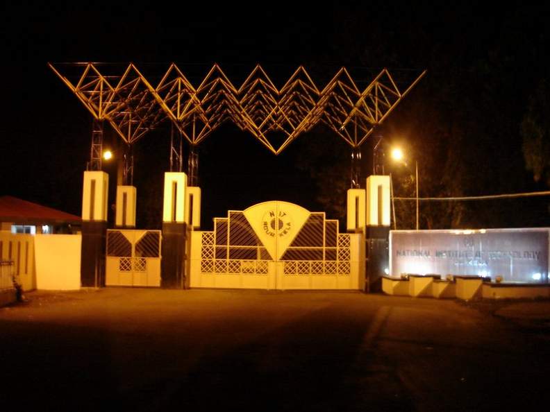 |